
ES Foundry Joins MIT Manufacturing Initiative With $1.5 Million Commitment – News and Statistics


Sep 21, 2026

ES Foundry, a U.S. business focused on bringing crystalline solar cell production back onshore, said on Sept. 21, 2026 that it has become a member of the Massachusetts Institute of Technology‘s Initiative for New Manufacturing. The company is putting $1.5 million into the initiative across three years as part of a fresh partnership aimed at bolstering American manufacturing.

According to the company, the tie-up will speed up its exploration of artificial intelligence-driven efficiency gains and sophisticated operating models, with the goal of keeping U.S. manufacturing globally competitive.

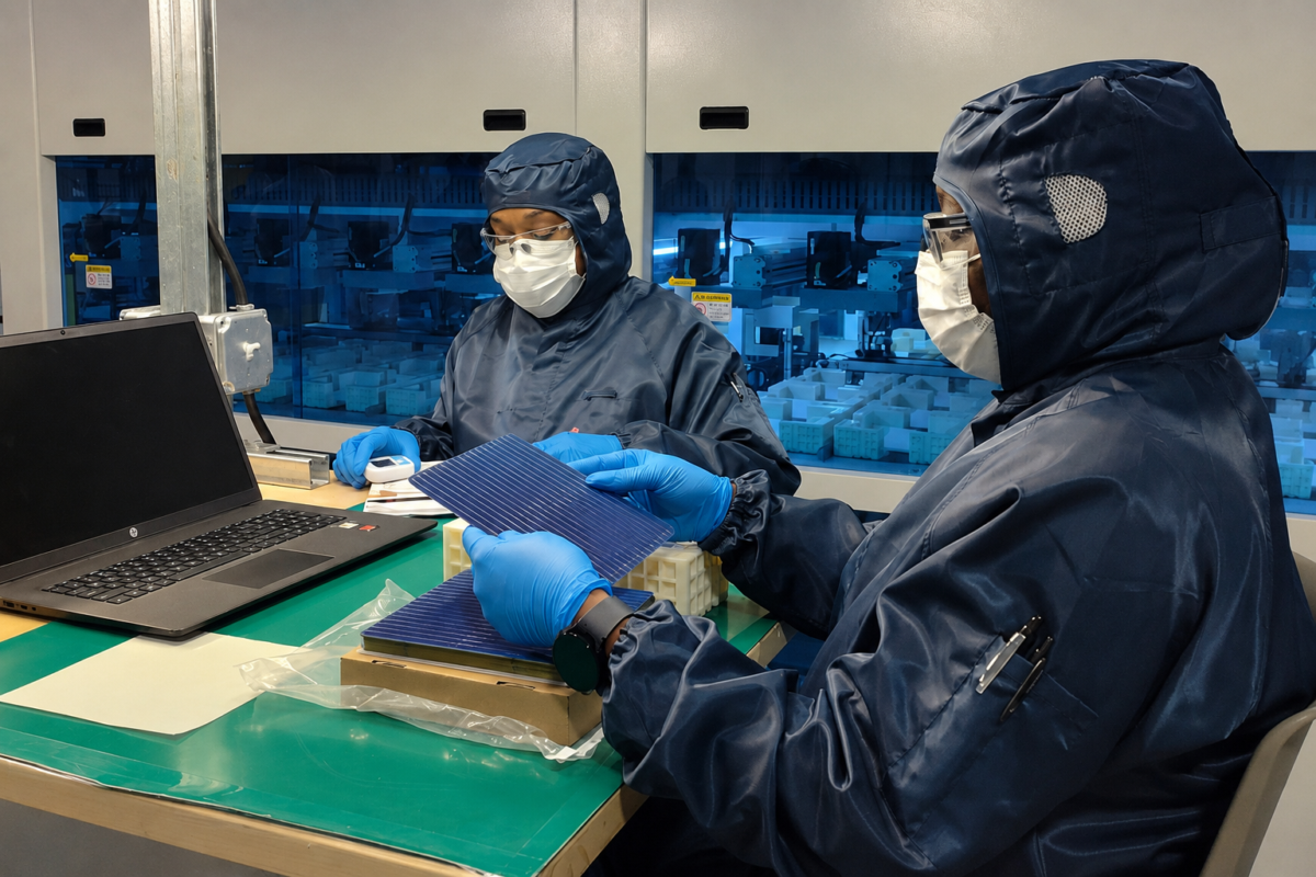
The move lands at a pivotal moment for ES Foundry’s expansion. In July, the company finished a 2 gigawatt enlargement of its Greenwood, South Carolina, plant, lifting total yearly solar cell production capacity to 3 gigawatts and backing over 400 advanced manufacturing positions.

Now that this capacity exists, ES Foundry said it is shifting attention past sheer manufacturing scale toward the technologies, workforce and operating methods that will decide whether American solar manufacturing can stay competitive over the long haul.

Alex Zhu, the company’s chief executive, said ES Foundry has invested substantially in restoring solar cell manufacturing to the United States, and that its pledge to the MIT initiative amounts to an investment in fortifying that manufacturing. Zhu noted that running at commercial scale daily provides a grounded perspective on where technology, automation and workforce development can have an impact, and that partnering with MIT offers a chance to investigate solutions to manufacturing difficulties and to devise fresh ideas and approaches.

Per the company, solar cells continue to be a crucial missing piece in the domestic photovoltaic supply chain. Although U.S. module manufacturing capacity has grown considerably, a large portion of the industry still relies on imported cells. ES Foundry said it was created to help alter that situation by making high-performance crystalline solar cells within the United States.

The Greenwood site turns out bifacial PERC solar cells for utility-scale, commercial and community solar uses. The finished expansion provides ES Foundry with a 3 gigawatt operating base where enhancements in production technology, automation, process control, workforce skills and factory efficiency can be deployed at commercial scale.

The $1.5 million pledge will underpin ES Foundry’s participation with the initiative and its wider efforts to tackle difficulties confronting modern manufacturers. Via the initiative, ES Foundry will collaborate with MIT faculty, researchers and students, along with manufacturers from other sectors, on subjects such as artificial intelligence on the factory floor, automated systems, cybersecurity, digital twins, continuous innovation and workforce development.

The partnership is intended to flow in both directions, with ES Foundry able to tap into fresh thinking from MIT while contributing the know-how of a manufacturer that is actively running and growing a highly technical production process in the United States.

Lionel Moss, general manager of operations at ES Foundry, said manufacturing difficulties become quite tangible when a factory operates around the clock. Moss said the company continually looks at ways to boost yield, productivity, equipment performance, processes and workforce capabilities, and that it has plenty to gain from the work at MIT while also offering Greenwood-derived experiences. He called that interchange the source of the collaboration’s value.

The Initiative for New Manufacturing unites manufacturers from various industries with MIT researchers, educators and students to address common production challenges. Since its 2025 launch, the initiative has broadened its efforts across manufacturing research, industry engagement, workforce development and entrepreneurship, with programs exploring areas from factory-floor artificial intelligence and automation to cybersecurity, digital twins and novel methods for cultivating manufacturing talent.

John Hart, a professor and head of the MIT Department of Mechanical Engineering who is faculty co-director of the initiative, said ES Foundry contributes a valuable perspective to the initiative and welcomed the company into the community.

ES Foundry said its participation in the initiative extends a wider push to build a lasting domestic solar cell manufacturing foundation. Having production capacity in the United States is a key initial step, and the company’s current focus is making sure U.S. solar cell manufacturing keeps advancing, innovating and competing as the industry expands.

Headquartered in South Carolina, ES Foundry portrays itself as speeding up the U.S. solar industry by onshoring crystalline solar cell manufacturing. Its Greenwood plant makes cells designed to satisfy the requirements of U.S. panel manufacturers and the supply chain needs of developers and engineering, procurement and construction firms. The company said it was purpose-built for Foreign Entity of Concern compliance and runs with entirely non-FEOC ownership, leadership and financing, guaranteeing transparent supply chains and verified eligibility for incentives, including the domestic content bonus.

Interactive table based on the Store Companies dataset for this report.

Sort: Rank
Sort: Company A-Z
Sort: Headquarters A-Z

#
Company
Headquarters
Focus
Scale
Note

1
First Solar
Tempe, Arizona
Solar cells (thin-film)
Large
Major US solar manufacturer

2
SunPower Corporation
San Jose, California
High-efficiency solar cells
Large
Residential & commercial solar

3
Cree LED (SMART Global Holdings)
Durham, North Carolina
LED components & lighting
Large
Former Cree LED business

4
Maxeon Solar Technologies
San Jose, California
Solar cells & panels
Large
Spin-off from SunPower

5
Luminus Devices
Fremont, California
LED components
Medium
Specialty & high-power LEDs

6
Bridgelux
Fremont, California
LED arrays & lighting
Medium
LED technology & solutions

7
Sundiode
Princeton, New Jersey
Semiconductor lasers & VCSELs
Small
Advanced photonics

8
Solaria
Fremont, California
High-efficiency solar cells
Medium
Residential solar panels

9
MiaSolé Hi-Tech Corp
Santa Clara, California
Flexible thin-film solar
Medium
CIGS solar technology

10
Heliene
Mountain Iron, Minnesota
Solar cells & modules
Medium
US & Canadian manufacturing

11
Silfab Solar
Bellingham, Washington
Solar cells & modules
Medium
North American manufacturing

12
Mission Solar Energy
San Antonio, Texas
Solar cells & modules
Medium
US-made solar panels

13
Qcells (Hanwha Q CELLS USA)
Irvine, California
Solar cell & panel manufacturing
Large
US operations of Korean parent

14
Aledia
Fremont, California
MicroLED technology
Small
3D architecture LEDs

15
Soraa
Fremont, California
GaN on GaN LEDs
Medium
High-quality lighting

16
Lumiode
New York, New York
Microdisplay LEDs
Small
High-brightness microdisplays

17
Glo
Nashville, Tennessee
UV-C LED technology
Small
Disinfection & purification

18
Suniva
Norcross, Georgia
Solar cells & modules
Medium
US crystalline silicon solar

19
Swift Solar
San Carlos, California
Perovskite solar cells
Small
Next-generation tandem cells

20
Tandem PV
San Jose, California
Perovskite-silicon solar
Small
Tandem cell technology

21
Brightspot Automation
Boulder, Colorado
LED testing & sorting
Small
Manufacturing equipment

22
SolarTech Universal
Livermore, California
Solar cell manufacturing
Small
Turnkey production lines

23
Arizona Sun
Chandler, Arizona
Solar cell & panel sales
Small
Distributor & assembler

24
GreenBrilliance
Sterling, Virginia
Solar panel integration
Medium
Residential & commercial

25
Lumileds
San Jose, California
LED components & automotive
Large
Former Philips business

26
Lighting Science Group
West Warwick, Rhode Island
LED lighting solutions
Medium
Specialty & horticultural

27
Energy Focus
Solon, Ohio
LED lighting products
Medium
Military & commercial

28
Crystal IS
Green Island, New York
UVC LEDs
Small
Aluminum nitride substrates

29
HexaTech
Morrisville, North Carolina
AlN substrates for LEDs
Small
Materials for UV LEDs

30
Kyocera AVX
Fountain Inn, South Carolina
LED components & optoelectronics
Large
US division of Kyocera


Free Training

Source link

US launches Foundry School to build advanced manufacturing workforce


The programme will train entrepreneurs, engineers, technicians, and industrial leaders through a 17-session advanced manufacturing curriculum.

The US launched the Foundry School on 3 September 2026 as a training programme for entrepreneurs, engineers, technicians, and industrial leaders to support the rebuilding of US manufacturing. Vice President J.D. Vance and Secretary of State Marco Rubio announced the programme at an event hosted by Under Secretary for Economic Affairs Jacob Helberg at the Donald J. Trump Institute of Peace.

Foundry School is being developed with Stanford University and seven other universities: Arizona State University, Georgia Institute of Technology, The Ohio State University, The Pennsylvania State University, the University of Kansas, Vanderbilt University, and Washington University in St. Louis. The programme will run 17 sessions across the eight campuses, with each session taught by founders and CEOs from advanced manufacturing enterprises in the United States and Pax Silica economies, including South Korea, Japan, Taiwan, and India.

The curriculum will be delivered in two phases. Seven regional sessions beginning in September 2026 will cover modern factory design, materials and supply chains, assembly-line engineering, plant economics, regulation and permitting, and workforce development at scale. A ten-session core programme at Stanford University beginning in January 2027 will cover advanced manufacturing capabilities including precision tooling, industrial automation, quality systems, new product introduction, digital manufacturing, capital equipment, energy, global site selection, and defence production.

Foundry School is a flagship initiative of Pax Silica, the Trump administration’s economic security partnership connecting governments, industry, and universities around critical supply chains and industrial capabilities underpinning the AI economy. The US Department of State estimates that American manufacturers will need 3.8 million skilled workers by 2033 across sectors including semiconductors, defence, and energy. The programme is intended to help close gaps in design and manufacturing capacity and connect students and workers directly with companies building and operating advanced manufacturing facilities.

Why does it matter?

Advanced manufacturing requires specialised technical and industrial skills as investment in areas such as semiconductors, energy, and defence expands. Bringing universities and industry leaders into a common training programme can connect workforce development with the practical requirements of manufacturing enterprises.

The programme also links skills development with industrial and economic security priorities. Its focus on both foundational and advanced manufacturing capabilities provides training across different stages of the manufacturing process, from factory design and supply chains to automation, digital manufacturing, and production.

Would you like to learn more about AI, tech, and digital diplomacy? If so, ask our Diplo chatbot!

Free Training

Source link

Foundry School Launched To Rebuild American Manufacturing


The Trump administration has launched a Foundry School, a training program for entrepreneurs, engineers, technicians, and industrial leaders to rebuild American manufacturing.

The launch of the training school was announced by Vice President J.D. Vance and Secretary of State Marco Rubio at an event held at the Donald J. Trump Institute of Peace.

They were joined by Under Secretary for Economic Affairs Jacob Helberg, presidents and senior leaders from the eight universities working to deliver the Foundry School curriculum and chief executives and company presidents from manufacturing and technology companies.

It is estimated that American manufacturers will need 3.8 million skilled workers by 2033 in semiconductors, defense, energy, and beyond. The State Department, working with Congress, plans to support the participation of Pax Silica economies in Foundry School and is working with Stanford University to develop the curriculum for U.S. and foreign participants. Foundry School will collaborate with Pax Silica economies to create opportunities for America and partners in industries critical to our nation’s economic security.

Foundry School is anchored in a first-of-its-kind advanced manufacturing curriculum developed by Stanford University that also features keystone lectures provided by seven universities. Stanford University has collaborated with Arizona State University, Georgia Institute of Technology, The Ohio State University, The Pennsylvania State University, the University of Kansas, Vanderbilt University, and Washington University in St. Louis. Across these eight campuses, the program will run 17 sessions, each taught by founders and CEOs from advanced manufacturing enterprises.

These industry leaders will be drawn from the United States and Pax Silica participants, including South Korea, Japan, Taiwan, and India, covering everything it takes to build and run a world-class manufacturing enterprise.

Foundry School is a flagship initiative of Pax Silica, the Trump Administration’s economic security partnership connecting governments, industry, and universities to strengthen the critical supply chains and industrial capabilities that underpin the AI economy. Foundry School connects students and workers directly with the companies building and operating advanced manufacturing facilities.

For comments and feedback contact: editorial@rttnews.com

Business News

Free Training

Source link

ES Foundry backs PERC amid US PV manufacturing shift to n-type


ES Foundry CEO Alex Zhu tells PV Tech Premium that the company’s strategy is centred on delivering commercially bankable US-made cells today, even as it prepares to transition from crystalline bifacial p-type passivated emitter rear contact (PERC) to a next-generation n-type technology.

The company recently completed a 2GW expansion of its solar cell manufacturing capacity in Greenwood, South Carolina, taking its total capacity to 3GW as it seeks to establish itself as one of the few large-scale crystalline silicon cell manufacturers producing and shipping product in the US.

Es Foundry began operations with its first 1GW of capacity in 2025. According to Zhu, the company expects to have the expanded capacity fully ramped by October.

For him, however, the significance of the expansion extends beyond the headline capacity figure. He argues that ES Foundry’s differentiation lies in having moved from announcements to actual production.

“In terms of actual production, we are the largest crystalline solar cell manufacturer in the US,” Zhu tells PV Tech Premium.

He contrasts this approach with what he describes as a US solar manufacturing landscape characterised by numerous large announcements, some of which have not translated into operating capacity.

That focus on delivering product is also central to ES Foundry’s technology strategy.

Why PERC? And what comes next?

Last year, energy market analyst Clean Energy Associates (CEA) said PERC solar PV technology was “all but obsolete” in Europe, with n-type tunnel oxide passivated contact (TOPCon), heterojunction (HJT) and back contact (BC) technologies having almost entirely displaced it in “many international markets”, driven by China’s manufacturing scale, lower prices and higher efficiency.

Yet while much of the global industry has moved on, US cell manufacturer ES Foundry is taking a different approach, betting on PERC as the foundation of its domestic manufacturing strategy — for now.

Zhu acknowledges that PERC does not offer the same efficiency potential as newer cell technologies. But he argues that efficiency is only one part of the equation for a new US manufacturing operation.

“The reason we chose PERC is that it is very reliable and has a robust process window,” he notes.

For ES Foundry, that maturity provides two important advantages. The first is bankability. Financial institutions and customers are already familiar with PERC, while some newer technologies have a shorter track record in commercial manufacturing.

“The whole banking industry are familiar with PERC,” Zhu says. “Whereas some of the new technologies in US have not been fully tested.”

The second advantage is manufacturing. The US is rebuilding a solar manufacturing workforce after years in which much of the global cell production base migrated to Asia. Zhu says the shortage of experienced engineers, operators and technicians makes manufacturing a mature technology with a relatively forgiving process window particularly valuable.

“Using PERC as a starting point is very good for us to train the local labour force without cause a significant loss of efficiency or reliability.”

PERC is therefore the starting point rather than the destination. Zhu says ES Foundry will eventually move from p-type to n-type technology, but the company has not yet decided which specific n-type architecture it will adopt.

“We will move to n-type technology. However, we haven’t decided which n-type technology we will go with because this depends on multiple things like IP issues, the supply chain, and equipment availability.”

For ES Foundry, the choice of technology is also an IP decision. Recent TOPCon disputes involving First Solar, JinkoSolar, Trina Solar, Maxeon and Canadian Solar underline the litigation risks facing manufacturers adopting the technology in the US.

Section 232 creates a two-sided effect

Earlier this month, US President Donald Trump introduced a 15% tariff on imports of polysilicon and its derivatives, alongside minimum import prices, under Section 232, with the measures set to take effect on 4 December 2026.

Experts, who recently spoke with PV Tech Premium, said the Section 232 measures could support established US manufacturers and upstream investment, but raise solar costs, weaken demand and potentially deter new capacity, a tension echoed by Zhu. He says the measures on polysilicon and related upstream materials will significantly increase ES Foundry’s wafer costs.

“Our current wafer cost is, for example, from 4 cents to 7 cents imported from overseas. And after that, our cost will increase to like 15 cents plus 2 cents tariffs. That’s a significant increase in our cost. And of course, that will eventually increase our price to ship to our customers. Anytime you increase the price, a customer will not like it, and your demand will reduce,” the CEO emphasises.

Having said that, Zhu says the higher cost of imported wafers could ultimately be offset by stronger demand for domestic-content modules as the price gap with imported products narrows.

For ES Foundry, therefore, Section 232 presents a balancing act: higher input costs on one side, but potentially stronger demand for its US-made cells on the other.

Zhu says domestic-content modules can benefit from an additional 10% investment tax credit, potentially reducing the overall cost of a solar project even where the domestic-content module itself carries a higher upfront price.

“Even a domestic content module by itself is more expensive, but when you’re calculating into the whole formula, the total project cost will reduce,” he says.

Zhu also points to the rapid growth of solar projects associated with AI data centres as another source of demand.

“We see so many more project developers selling their projects to support the growth of AI data centres. At the same time, those customers also require domestic content because that will reduce the overall costs.”

The opportunity extends beyond cells. As domestic-content requirements increase, Zhu expects module manufacturers and their suppliers to look increasingly at other components, including junction boxes, EVA, ribbons and frames, to maximise the domestic contribution of their products.

The One Big Beautiful Bill Act (OBBBA) and evolving trade measures are therefore becoming important parts of the commercial landscape in which ES Foundry operates.

Building the US cell supply chain and the workforce to support it

For ES Foundry, scaling US cell manufacturing goes beyond adding capacity: the company still faces gaps in both its upstream supply chain and local workforce.

The company currently sources Chinese and non-Chinese polysilicon, with wafers produced in Southeast Asia, while US-made P-type wafers are not yet part of its supply chain.

For now, however, the company is focused on ramping its cell operations rather than pursuing backward integration into wafer manufacturing or forward integration into modules.

The workforce presents another challenge. Zhu says ES Foundry is training locally but continues to see a significant skills gap, prompting partnerships with MIT’s Initiative for New Manufacturing and a local community college in Greenwood.

“We’re doing a lot of training to train our local force, but there’s a significant gap,” he says. The training programme is intended to accelerate the development of workers capable of supporting both the current factory and future manufacturing expansion.

In the near term, ES Foundry appears confident that demand will support its existing 3GW annual nameplate capacity, with off-take agreements extending through 2028.

Zhu acknowledges that higher interest rates and interconnection delays could weigh on US solar demand, but says customers can shift delayed projects elsewhere.

“Most of our customers have multiple projects on hand, so even if some are delayed, they can easily shift to other projects.”

For ES Foundry, the immediate priority is therefore clear: establish reliable cell production while building the supply chain and workforce needed for its next phase of growth.

Free Training

Source link